Search
communications
Vortex Radiometer for Wireless Communications
The Vortex Radiometer (VR) creates concentric, annular antenna beam patterns that measure sky-noise temperature. Annular antenna patterns are created by imparting orbital angular momentum into the electric field received by the antenna using spiral phase plates placed in front of the antenna aperture, generating multiple radiometer channels. Data points are then collected by plotting the measured noise temperature of each radiometer channel as a function of time. Noise temperature increases as a noise source (e.g., weather-related noise, signal interference, etc.) traverses the antenna beam patterns. An algorithm is then used to correlate noise temperature peaks in adjacent beams and to determine when a fade will occur, how long the fade will last, and how intense the fade will be. With this information, effective and efficient strategies can be implemented using cognitive communication and antenna systems to autonomously select the optimum fade-mitigation technique and parameter (e.g., increasing the transmission power, adjusting the modulation and/or coding scheme, etc.).
NASA's VR system has been prototyped, including the radiometer device and the algorithm for characterizing noise sources based on VR data. Simulations have shown that a VR system can instruct an existing cognitive antenna to switch between Ka- and X-Band communications in order to avert interference from small diameter noise sources.
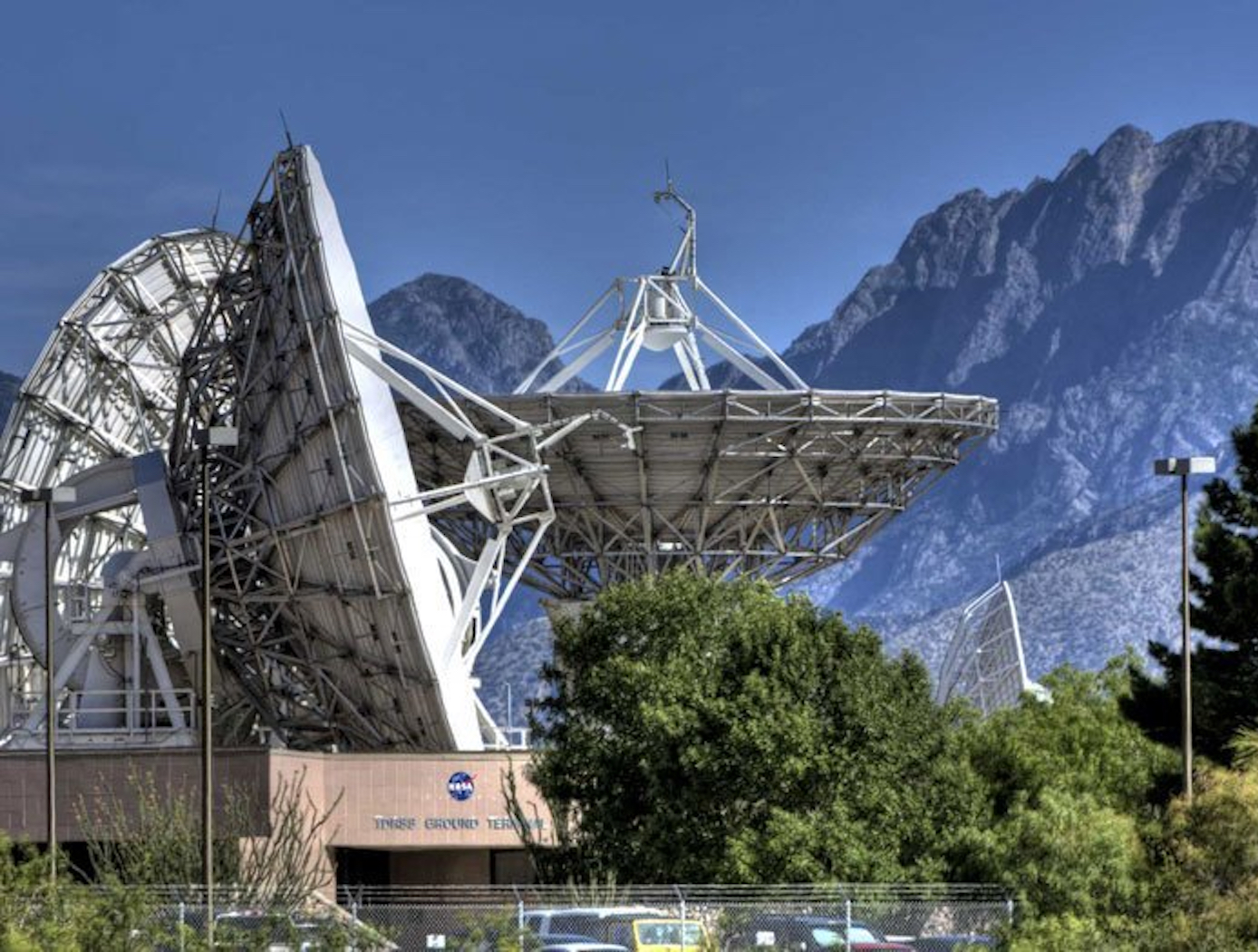
Any high-performance communication systems operating in RF or optical frequencies may benefit from NASA's VR capabilities.
Communications

Integrated-Photonic Electromagnetic Signal Detector
NASA’s ESD is a small form-factor electromagnetic signal detector fabricated on a photonic crystal substrate (e.g., silicon-on-insulator wafer, III-V platform). It integrates a (1) miniature on-chip antenna (e.g., microstrip antenna) aligned to the desired operational frequency, (2) 2-D photonic crystal, and (3) electro-optic polymer (located on the photonic crystal).
At the heart of the detector is the 2D photonic crystal. Using an array of carefully sized pores or “nano-cavities,” a waveguide is formed that governs the crystal’s optical transmission properties. An electro-optic polymer (a material that shifts its refractive index in response to external electric fields) is used to coat the photonic crystal. The combination of the 2D photonic crystal and EO polymer make up the resonator.
A compact antenna with separate active feed and ground regions is placed near the photonic crystal, creating a gap through which the electromagnetic signal couples to the photonic crystal structure. Under normal conditions (no external signal), the EO polymer’s refractive index remains unchanged, producing a stable resonant notch in the device’s optical transmission. When the antenna intercepts an electromagnetic wave, the resulting electric field modifies the EO polymer’s refractive index, causing a measurable shift in the resonator’s optical output. By monitoring this shift, a photodetector can accurately determine the presence and magnitude of the incoming electromagnetic wave.
NASA’s low SWaP-C, high precision ESD can be adapted for use in a variety of systems including remote sensing instruments (e.g., radiometers, spectrometers), transceivers for 5G communications networks, and other electromagnetic signal detection applications. The invention is available for patent licensing.

