Simplified Complimentary Metal-oxide-semiconductor Manufacturing Technique
manufacturing
Simplified Complimentary Metal-oxide-semiconductor Manufacturing Technique (LAR-TOPS-304)
Unique deposition process for CMOS manufacturing eliminating photoresists, UV exposure and other steps - Applicable for 3D transistors
Overview
Current microfabrication methods are well established for processing of Si-based complementary metal-oxide-semiconductor (CMOS) and only get more complex with each iteration. This is especially true with 3D transistors that require very selective placement and selective removal of materials required to reach a working product.
However, with NASA's newly developed masking and deposition processes, photoresists, UV exposures and selective etching can be eliminated, with metal removal reduced to only planarization. This revised process reduces the total material and time requirements drastically when compared to current standards.
These advancements offer the benefits of increasing total possible throughput while simultaneously reducing manufacturing cost per unit.
The Technology
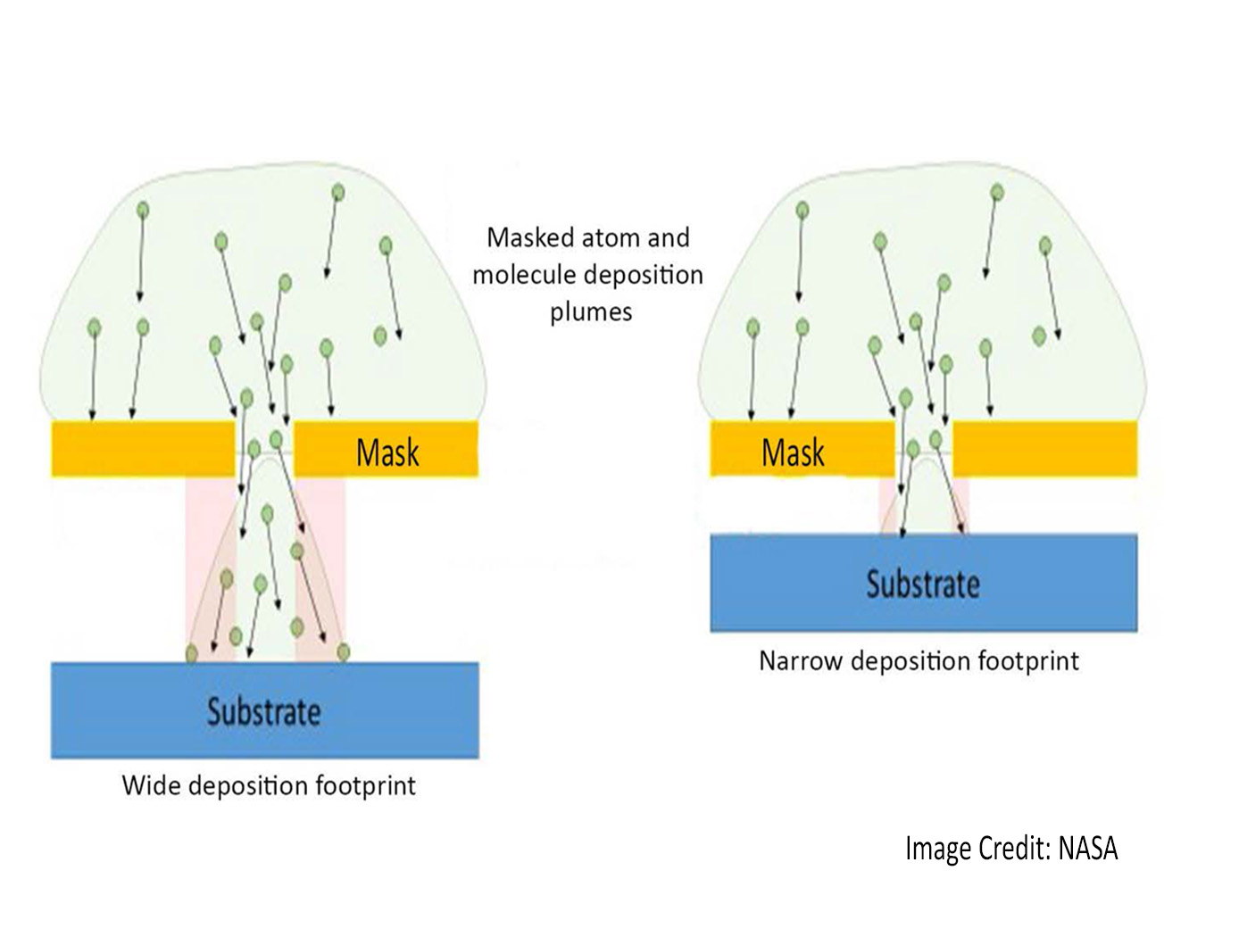
This innovation represents an alternative method to skip several of the conventional fabrication steps, using a mask designed to allow molecules in a sputtering plume to pass through openings engineered in the mask. This causes material to go where desired, without photoresist, and without selective etching, thus simplifying the process, reducing cost, chemical waste; and increasing throughput.
This method masks areas that do not need deposited material, causing local deposition instead. The shape and size are within tolerance. No etching steps, no photoresist patterning, and no metal removal is necessary. Other than planarization, selective deposition has replaced every step in the conventional process, accomplishing the same result in 8 steps instead of 19.
The technology can be easily used to fabricate custom chips and specialized sensors and devices that use the group III-V and II - VI semiconductor materials.

Benefits
- Shortens the patterning process for deposition, skipping the need for photoresist and UV exposure
- Cost is reduced
- Environmental impact is reduced from less chemical disposal
- Less material waste from etching away undesirable deposition
- Most effective for fabrication process for group III-V and II-VI semiconductors which do not have proper gate oxides
- Effective for thick film processing
Applications
- Semiconductors
- Computer equipment
- Telecommunications equipment
- Wireless communications
- Automotive applications
- Electronic imaging / optoelectronics
- Medical imaging
Similar Results

Novel Process to Create Structured Membrane Films for Micromachining Applications
The technology is an innovative process for creating metal-patterned, structured membranes for micromachining applications. The method uses potassium hydroxide to remove silicon, in combination with XHRiC. Hafnium metal is first patterned onto a silicon nitride wafer, which serves as the starting substrate. XHRiC is then applied to the wafer, followed by patterning with photoresist and etching using O2 plasma to define cut slots in the membrane. The photoresist is then removed.
Next, the wafer is bonded to a Pyrex carrier wafer with wax, and the backside of the silicon nitride is patterned and reactive-ion etched. The wafer is then placed in hot potassium hydroxide for 16 hours to remove the silicon layer, creating a silicon nitride membrane. The wafer is subsequently placed in acetone to dissolve the wax. The wafer is resecured to the Pyrex carrier wafer, and the topside of the silicon nitride membrane is subjected to reactive-ion etching. Finally, the XHRiC layer is removed using O2 plasma, and the Pyrex handle wafer is released, resulting in a metal-patterned silicon nitride membrane with cut slots.
This novel process supports the creation of structured membranes with a wide range of applications in MEMS fabrication. The use of XHRiC as a patterned hard mask and/or etch protection material enables its application in various MEMS devices. The process can be used to fabricate cut membranes, micro/nano structures, and ultra-thin films for device applications, making it an excellent candidate for MEMS foundry companies and accelerometer manufacturers. It has reached a Technology Readiness Level (TRL) 5 (component validation in a relevant environment) and is now available for patent licensing.

Ultra-low Reflectivity Black Silicon Pupil Masks
Fabrication of NASA's pupil mask begins with the preparation of a silicon wafer, which serves as the foundation for the black silicon structure. The wafer undergoes ion beam figuring (IBF), a non-contact technique that precisely removes surface irregularities at the nanometer scale. This process ensures that the silicon surface is diffraction-limited, eliminating errors that could degrade optical performance. Once the wafer is polished to the required precision, it is then processed lithographically to define the mask pattern, creating reflective and absorptive regions essential for controlling light propagation.
To achieve the desired high absorption characteristics, the lithographically patterned wafer undergoes cryogenic etching, a sophisticated process that transforms the silicon surface into a highly textured, black silicon structure. This method utilizes a controlled plasma environment with sulfur hexafluoride (SF6) and oxygen to etch the surface at cryogenic temperatures. The process is carefully optimized by adjusting parameters such as gas flow rates, chamber pressure, ion density, and etch duration, leading to the formation of high-aspect-ratio nanostructures on the silicon substrate. These structures, resembling a dense “forest” of silicon nanospikes, trap and diffuse incoming light, drastically reducing specular reflection. The resulting surface exhibits an ultra-low reflectivity that is orders of magnitude lower than conventional polished silicon.
By leveraging NASA’s cutting-edge fabrication technique, the newly developed black silicon pupil mask offers a powerful solution for high-contrast astronomical imaging. Its ability to minimize scattered light and enhance optical contrast makes it an ideal component for space telescopes tasked with directly imaging exoplanets as well as other applications requiring ultra low reflectivity systems.

Reduced PIC fabrication cost by one-step method
The new fabrication method is an electron lithography scheme enabling monolithic integration of multiple photonic devices on a single PIC. The technology was demonstrated by integrating both a widely-tunable distributed Bragg reflector (DBR) and distributed feedback (DFB) lasers on the same substrate. By controlling the central gap width and etch depth along the laser mirror length (shown in the figure below) the reflectivities can be tuned and the desired laser characteristics can be achieved without additional lithography cycles.
Initially demonstrated on an indium phosphide substrate with DBR and DFB elements, the platform technology shows promise for various other materials and devices like III-V and II-VI semiconductors, silicon-on-insulator (SOI), and planar lightwave circuits (PLCs). With this versatility, the invention described here can streamline PIC production across diverse applications.
Proof-of-concept results showcase the lithographic technique’s ability to produce high-performance photonic devices with side-mode suppression ratios over 50 dB (figure on the right) and output powers exceeding 5 mW. These metrics, combined with the lithographic simplicity, highlight the technology’s potential to reduce costs and accelerate PIC manufacturing. Please note that NASA does not manufacture products itself for commercial scale.

Biomarker Sensor Arrays for Microfluidics Applications
This invention provides a method and system for fabricating a biomarker sensor array by dispensing one or more entities using a precisely positioned, electrically biased nanoprobe immersed in a buffered fluid over a transparent substrate. Fine patterning of the substrate can be achieved by positioning and selectively biasing the probe in a particular region, changing the pH in a sharp, localized volume of fluid less than 100 nm in diameter, resulting in a selective processing of that region. One example of the implementation of this technique is related to Dip-Pen Nanolithography (DPN), where an Atomic Force Microscope probe can be used as a pen to write protein and DNA Aptamer inks on a transparent substrate functionalized with silane-based self-assembled monolayers. But it would be recognized that the invention has a much broader range of applicability. For example, the invention can be applied to formation of patterns using biological materials, chemical materials, metals, polymers, semiconductors, small molecules, organic and inorganic thins films, or any combination of these.

Solar Powered Carbon Dioxide (CO2) Conversion
This technology consists of a photoelectrochemical cell composed of thin metal oxide films. It uses sunlight (primarily the ultraviolet (UV), visible and Infrared (IR) portions)) and inexpensive titanium dioxide composites to perform the reaction. The device can be used to capture carbon dioxide produced in industrial processes before it is emitted to the atmosphere and convert it to a useful fuel such as methane. These devices can be deployed to the commercial market with low manufacturing and materials costs. They can be made extremely compact and efficient and used in sensor and detector applications.

