Search
Information Technology and Software

Additive Manufacturing Model-based Process Metrics (AM-PM)
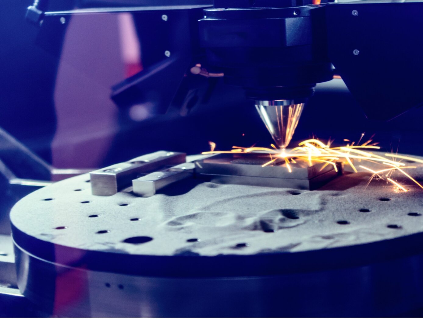
Modeling additive manufacturing processes can be difficult due to the scale difference between the active processing point (e.g., a sub-millimeter melt pool) and the part itself. Typically, the tools used to model these processes are either too computationally intensive (due to high physical fidelity or inefficient computations) or are focused solely on either the microscale (e.g., microstructure) or macroscale (e.g., cracks). These pitfalls make the tools unsuitable for fast and efficient evaluations of additive manufacturing build files and parts.
Failures in parts made by laser powder bed fusion (L-PBF) often come when there is a lack of fusion or overheating of the metal powder that causes areas of high porosity. AM-PM uses a point field-based method to model L-PBF process conditions from either the build instructions (pre-build) or in situ measurements (during the build). The AM-PM modeling technique has been tested in several builds including a Ti-6Al-4V test article that was divided into 16 parts, each with different build conditions. With AM-PM, calculations are performed faster than similar methods and the technique can be generalized to other additive manufacturing processes.
The AM-PM method is at technology readiness level (TRL) 6 (system/subsystem model or prototype demonstration in a relevant environment) and is available for patent licensing.
manufacturing

Additively Manufactured Propulsion Catalysts
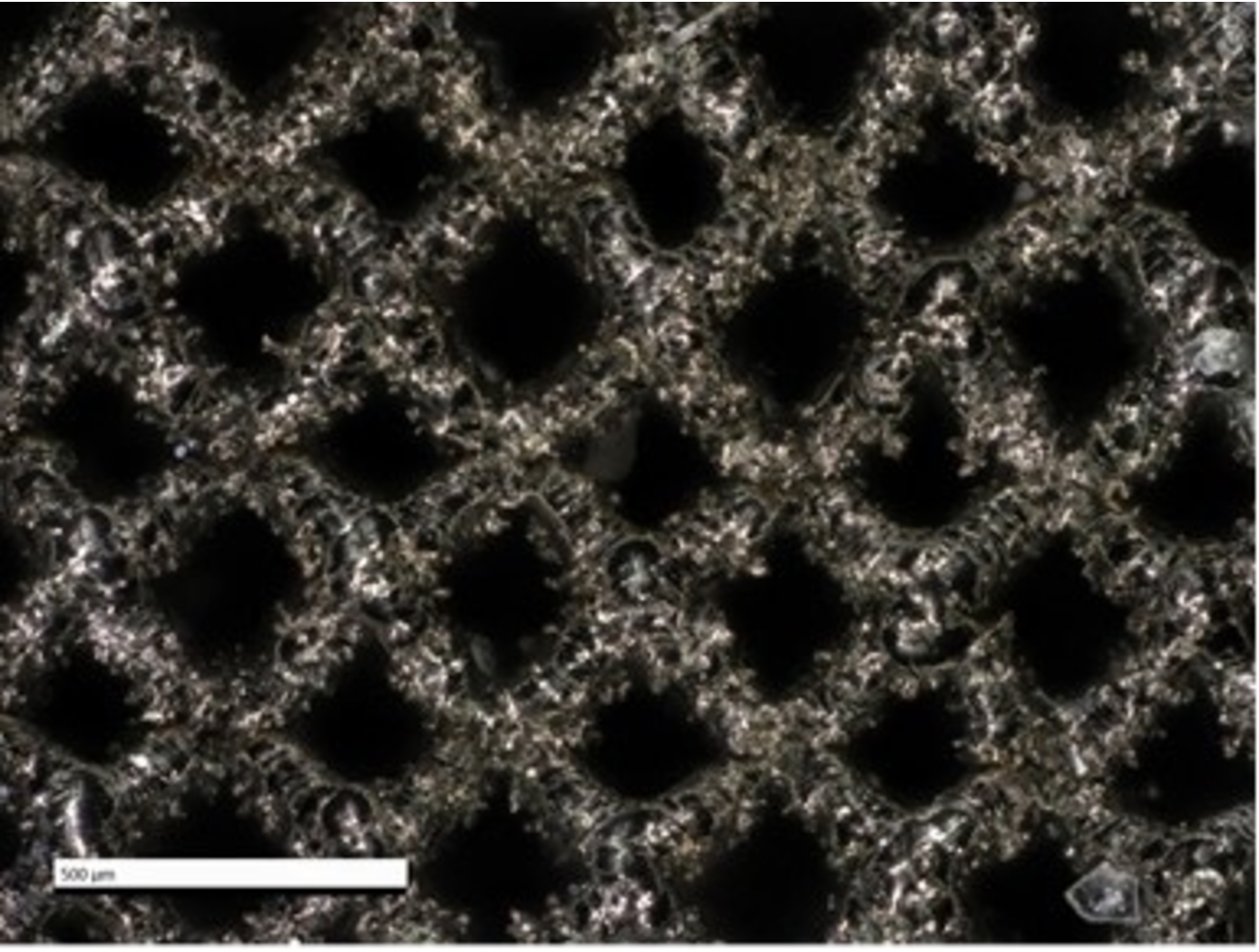
Working with EOS, a market leader in additive manufacturing (AM) technology, NASA has pioneered the use of AM to achieve improved performance and cost reduction of propulsion catalyst systems. As mentioned above, conventional mono-propulsion catalysts are comprised of ceramic or graphite foams, which possess thousands of irregular pores with non-uniform size and distribution. Due to the lack of granular control in the manufacturing process, such foams are limited in terms of feasible designs. These foams also exhibit anisotropic mechanical properties and inconsistent fluid flow behavior. Furthermore, such catalysts are produced by a limited number of vendors, constraining availability and inflating cost. As with several other aerospace structures, AM of mono-propulsion catalysts enables increased manufacturing capabilities (e.g., granular geometric control, repeatability) while reducing cost and lead time.
NASA and EOS leveraged AM to generate ultra-fine lattice structures repeating unit cells with ligament thickness as small as 100 microns to replace coated ceramic or graphite foam catalysts. These AM lattice structures offer several advantages including increased control of structure topology, unconstrained designed flexibility, improved compressive strength, and fluid flow optimization all printed into a single component from a preferred refractory platinum metal. Granular control of structure topology allows for tailored percent relative density (%RD), which in turn allows manufacturers to control the mechanical and fluid flow properties of the final catalyst structure. In other words, NASAs AM ultra-fine lattice catalyst structures significantly improve upon the drawbacks of conventional catalysts by offering a higher degree of control over the structure, enabling the generation of catalysts with customized material properties. In addition, the use of AM ensures the catalysts exhibit high spatial symmetry and can be generated in a repeatable (non-stochastic) manner, all while reducing cost and lead times.
While NASA and EOS' ultra-fine lattice structures were originally developed for mono-propellant systems (e.g., green propellant thruster catalysts), the same structures and manufacturing technologies can be applied to liquid or gas permeable rigid materials, evaporative film cooling heat exchangers, filtering, and other applications.
Sensors

Advanced Thermal Inspection with Pulsed Light Emitting Diodes (PLED) Technology
NASA’s PLED thermal inspection system consists of an array of high- powered LED chips configured to deliver controlled pulses of visible light. The system includes 8 LED chip arrays, mounted on an aluminum heat sink and housed in a hood configuration. The inspection hood is specially designed with filters to prevent internal reflections. The LEDs are powered by regulated power supplies and controlled via a computer interface that synchronizes heat pulses with an infrared camera. An acrylic filter is placed over the LEDs to block residual infrared radiation, ensuring that only visible light reaches the target surface. The system’s infrared camera, operating in the mid-wave infrared (MWIR) range does not detect the visible light and captures the transient thermal response of the material, allowing for precise defect detection. By eliminating the need for high-intensity broadband infrared sources, the PLED system provides a cleaner and more accurate thermal response, particularly for unpainted metals and additively manufactured (AM) components.
Performance validation of the PLED system has demonstrated significant advantages over traditional flash thermography. In tests on aluminum samples with material loss and AM Ti-6Al-4V metal specimens, the PLED system successfully detected defects with superior contrast and no heat source reflections. Principal Component Analysis (PCA) applied to PLED inspection data revealed clearer defect indications compared to flash-based methods, which introduced unwanted artifacts due to transient reflections. Additionally, the PLED system enabled quantitative thermal diffusivity measurements, offering a new approach to single-sided material characterization.
NASA's PLED thermal inspection technology is available for patent licensing. Potential applications include corrosion detection in aerospace components, quality control of AM metal parts, structural health monitoring of industrial materials, and more.


