Search
environment

Miniaturized Laser Heterodyne Radiometer
This instrument uses a variation of laser heterodyne radiometer (LHR) to measure the concentration of trace gases in the atmosphere by measuring their absorption of sunlight in the infrared. Each absorption signal is mixed with laser light (the local oscillator) at a near-by frequency in a fast photoreceiver. The resulting beat signal is sensitive to changes in absorption, and located at an easier-to-process RF frequency. By separating the signal into a RF filter bank, trace gas concentrations can be found as a function of altitude.
sensors

Detection Of Presence Of Chemical Precursors
These needs are met by this invention, which provide easy stem and associated method for detecting one or more chemical precursors (components) of a multi-component explosive compound. Different carbon nanotubes (CNTs) are loaded (by doping, impregnation, coating, or other functionalization process) for detecting of different chemical substances that are the chemical precursors, respectively, if these precursors are present in a gas to which the CNTs are exposed. After exposure to the gas, a measured electrical parameter (e.g. voltage or current that correlate to impedance, conductivity, capacitance, inductance, etc.) changes with time and concentration in a predictable manner if a selected chemical precursor is present, and will approach an asymptotic value promptly after exposure to the precursor.
The measured voltage or current are compared with one or more sequence soft heir reference values for one or more known target precursor molecules, and a most probable concentration value is estimated for each one, two, or more target molecules. An error value is computed, based on differences of voltage or current for the measured and reference values, using the most probable concentration values. Where the error value is less than a threshold, the system concludes that the target molecule is likely. Presence of one, two, or more target molecules in the gas can be sensed from a single set of measurements.
sensors
Gas Composition Sensing Using Carbon Nanotube Arrays
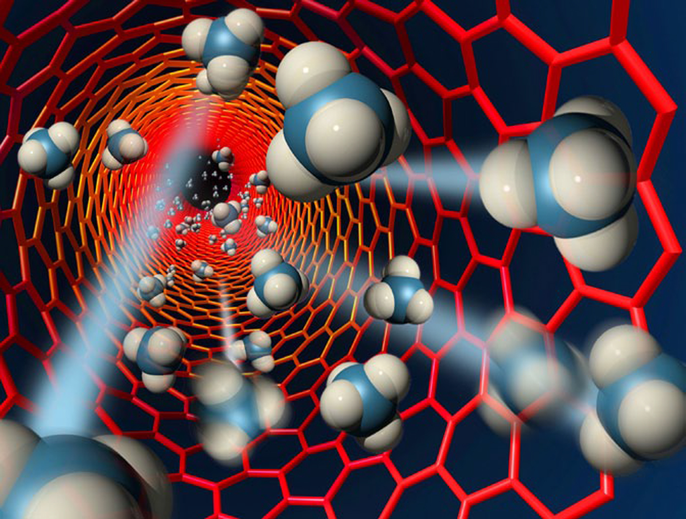
An array of carbon nanotubes (CNTs) in a substrate is connected to a variable-pulse voltage source. The CNT tips are spaced appropriately from the second electrode maintained at a constant voltage. A sequence of voltage pulses is applied and a pulse discharge breakdown threshold voltage is estimated for one or more gas components, from an analysis of the current-voltage characteristics. Each estimated pulse discharge breakdown threshold voltage is compared with known threshold voltages for candidate gas components to estimate whether at least one candidate gas component is present in the gas. The procedure can be repeated at higher pulse voltages to estimate a pulse discharge breakdown threshold voltage for a second component present in the gas.
The CNTs in the gas sensor have a sharp (low radius of curvature) tip; they are preferably multiwall carbon nanotubes (MWCNTs) or carbon nanofibers (CNFs), to generate high-strength electrical fields adjacent to the current collecting plate, such as a gold plated silicon wafer or a stainless steel plate for breakdown of the gas components with lower voltage application and generation of high current. The sensor system can provide a high-sensitivity, low-power-consumption tool that is very specific for identification of one or more gas components. The sensors can be multiplexed to measure current from multiple CNT arrays for simultaneous detection of several gas components.
sensors
Multidimensional Damage Detection System
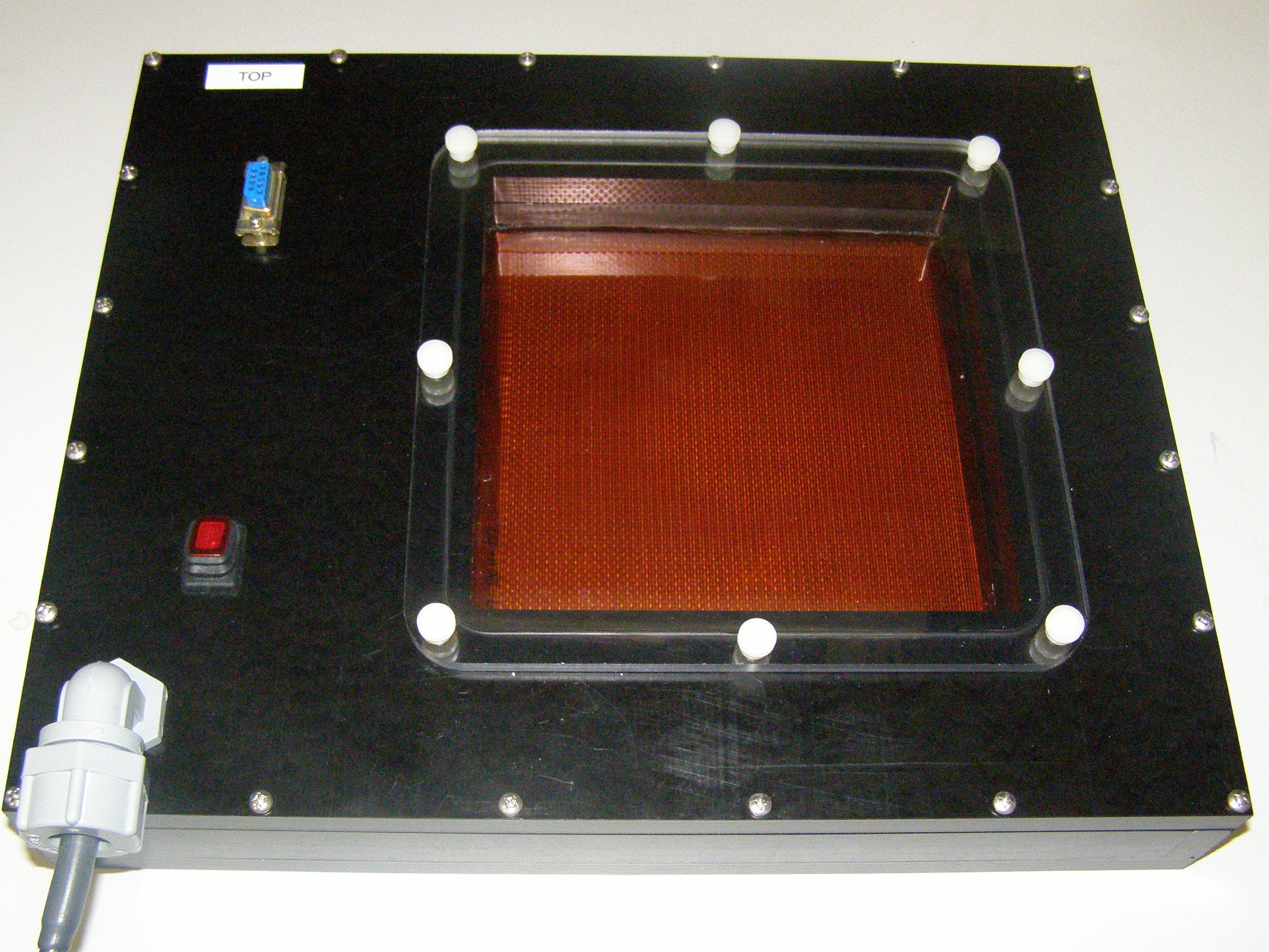
The Damage Detection System consists of layered composite material made up of two-dimensional thin film damage detection layers separated by thicker, nondetection layers, coupled with a detection system. The damage detection layers within the composite material are thin films with a conductive grid or striped pattern. The conductive pattern can be applied on a variety of substrates using several different application methods. The number of detection layers in the composite material can be tailored depending on the level of damage detection detail needed for a particular application. When damage occurs to any detection layer, a change in the electrical properties of that layer is detected and reported. Multiple damages can be detected simultaneously, providing real-time detail on the depth and location of the damage.
The truly unique feature of the System is its flexibility. It can be designed to gather as much (or as little) information as needed for a particular application using wireless communication. Individual detection layers can be turned on or off as necessary, and algorithms can be modified to optimize performance. The damage detection system can be used to generate both diagnostic and prognostic information related to the health of layered composite structures, which will be essential if such systems are utilized to protect human life and/or critical equipment and material.
sensors
Biomarker Sensor Arrays for Microfluidics Applications
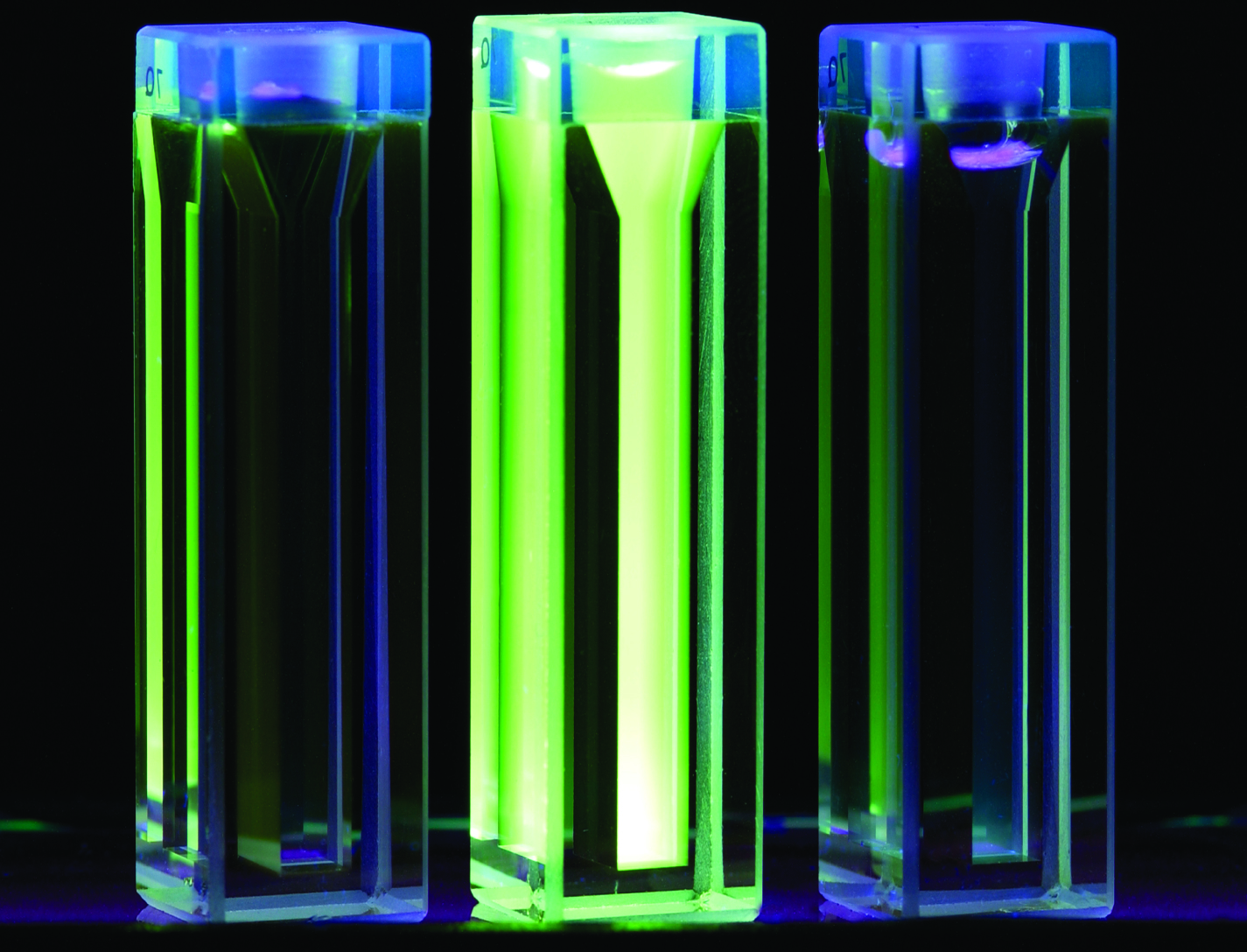
This invention provides a method and system for fabricating a biomarker sensor array by dispensing one or more entities using a precisely positioned, electrically biased nanoprobe immersed in a buffered fluid over a transparent substrate. Fine patterning of the substrate can be achieved by positioning and selectively biasing the probe in a particular region, changing the pH in a sharp, localized volume of fluid less than 100 nm in diameter, resulting in a selective processing of that region. One example of the implementation of this technique is related to Dip-Pen Nanolithography (DPN), where an Atomic Force Microscope probe can be used as a pen to write protein and DNA Aptamer inks on a transparent substrate functionalized with silane-based self-assembled monolayers. But it would be recognized that the invention has a much broader range of applicability. For example, the invention can be applied to formation of patterns using biological materials, chemical materials, metals, polymers, semiconductors, small molecules, organic and inorganic thins films, or any combination of these.
sensors
Electrical Response Using Nanotubes on a Fibrous Substrate
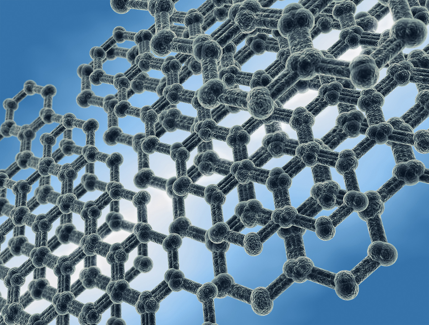
A resistor-type sensor was fabricated which has a network of cross-linked SWCNTs with purity over 99%. An ordinary cellulose paper used for filtration was employed as the substrate. The filter paper exhibits medium porosity with a flow rate of 60 mL/min and particle retention of 5-10m. The roughness and porosity of the papers are attractive because they increase the contact area with the ambient air and promote the adhesion to carbon nanotubes. The SWCNTs were functionalized with carboxylic acid (COOH) to render them hydrophilic, thus increasing the adhesion with the substrate. The functionalized SWCNTs were dispersed in dimethylformamide solution. The film composed of networks of cross-linked CNTs was formed using drop-cast coating followed by evaporation of the solvent. Adhesive copper foil tape was used for contact electrodes. Our sensors outperformed the oxide nanowire-based humidity sensors in terms of sensitivity and response/recovery times.
optics

Non-Scanning 3D Imager
NASA Goddard Space Flight Center's has developed a non-scanning, 3D imaging laser system that uses a simple lens system to simultaneously generate a one-dimensional or two-dimensional array of optical (light) spots to illuminate an object, surface or image to generate a topographic profile.
The system includes a microlens array configured in combination with a spherical lens to generate a uniform array for a two dimensional detector, an optical receiver, and a pulsed laser as the transmitter light source. The pulsed laser travels to and from the light source and the object. A fraction of the light is imaged using the optical detector, and a threshold detector is used to determine the time of day when the pulse arrived at the detector (using picosecond to nanosecond precision). Distance information can be determined for each pixel in the array, which can then be displayed to form a three-dimensional image.
Real-time three-dimensional images are produced with the system at television frame rates (30 frames per second) or higher.
Alternate embodiments of this innovation include the use of a light emitting diode in place of a pulsed laser, and/or a macrolens array in place of a microlens.
information technology and software
The Hilbert-Huang Transform Real-Time Data Processing System
The present innovation is an engineering tool known as the HHT Data Processing System (HHTDPS). The HHTDPS allows applying the Transform, or 'T,' to a data vector in a fashion similar to the heritage FFT. It is a generic, low cost, high performance personal computer (PC) based system that implements the HHT computational algorithms in a user friendly, file driven environment. Unlike other signal processing techniques such as the Fast Fourier Transform (FFT1 and FFT2) that assume signal linearity and stationarity, the Hilbert-Huang Transform (HHT) utilizes relationships between arbitrary signals and local extrema to find the signal instantaneous spectral representation.
Using the Empirical Mode Decomposition (EMD) followed by the Hilbert Transform of the empirical decomposition data, the HHT allows spectrum analysis of nonlinear and nonstationary data by using an engineering a-posteriori data processing, based on the EMD algorithm. This results in a non-constrained decomposition of a source real value data vector into a finite set of Intrinsic Mode Functions (IMF) that can be further analyzed for spectrum interpretation by the classical Hilbert Transform.
The HHTDPS has a large variety of applications and has been used in several NASA science missions.
NASA cosmology science missions, such as Joint Dark Energy Mission (JDEM/WFIRST), carry instruments with multiple focal planes populated with many large sensor detector arrays with sensor readout electronics circuitry that must perform at extremely low noise levels.
A new methodology and implementation platform using the HHTDPS for readout noise reduction in large IR/CMOS hybrid sensors was developed at NASA Goddard Space Flight Center (GSFC). Scientists at NASA GSFC have also used the algorithm to produce the first known Hilbert-Transform based wide-field broadband data cube constructed from actual interferometric data.
Furthermore, HHT has been used to improve signal reception capability in radio frequency (RF) communications.
This NASA technology is currently available to the medical community to help in the diagnosis and prediction of syndromes that affect the brain, such as stroke, dementia, and traumatic brain injury.
The HHTDPS is available for non-exclusive and partial field of use licenses.
manufacturing
.jpg)
Interim, In Situ Additive Manufacturing Inspection
The in situ inspection technology for additive manufacturing combines different types of cameras strategically placed around the part to monitor its properties during construction. The IR cameras collect accurate temperature data to validate thermal math models, while the visual cameras obtain highly detailed data at the exact location of the laser to build accurate, as-built geometric models. Furthermore, certain adopted techniques (e.g., single to grouped pixels comparison to avoid bad/biased pixels) reduce false positive readings.
NASA has developed and tested prototypes in both laser-sintered plastic and metal processes. The technology detected errors due to stray powder sparking and material layer lifts. Furthermore, the technology has the potential to detect anomalies in the property profile that are caused by errors due to stress, power density issues, incomplete melting, voids, incomplete fill, and layer lift-up. Three-dimensional models of the printed parts were reconstructed using only the collected data, which demonstrates the success and potential of the technology to provide a deeper understanding of the laser-metal interactions. By monitoring the print, layer by layer, in real-time, users can pause the process and make corrections to the build as needed, reducing material, energy, and time wasted in nonconforming parts.
Sensors
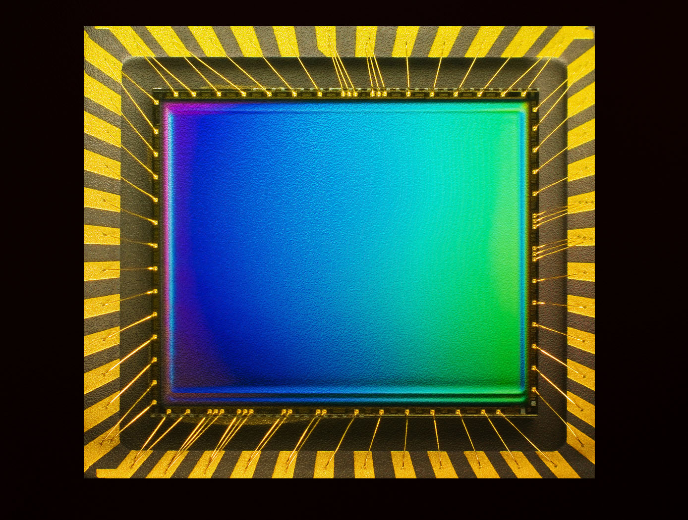
Gas Sensors Based on Coated and Doped Carbon Nanotubes
A typical sensor device includes a set of interdigitated microelectrodes fabricated by photolithography on silicon wafer or an electrically insulating substrate. In preparation for fabricating the SWCNT portion of such a sensor, a batch of treated (coated or doped) SWCNTs is dispersed in a solvent. The resulting suspension of SWCNTs is drop-deposited or injected onto the area containing the interdigitated electrodes. As the solvent evaporates, the SWCNTs form a mesh that connects the electrodes. The density of the SWCNTs in the mesh can be changed by varying the concentration of SWCNTs in the suspension and/or the amount of suspension dropped on the electrode area. To enable acquisition of measurements for comparison and to gain orthogonality in the sensor array, undoped SWCNTs can be similarly formed on another, identical set of interdigitated electrodes. Coating materials tested so far include chlorosulfonated polyethylene. Dopants that have been tested include Pd, Pt, Au, Cu and Rh nanoparticle clusters. To date, the sensor has been tested for NO2, NH3, CH4, Cl2, HCl, toluene, benzene, acetone, formaldehyde and nitrotoulene.


