Search
PATENT PORTFOLIO
Electrical and Electronics
NASA's portfolio of electrical and electronics technologies represents a vast array of innovative solutions for a wide range of applications. Whether you are looking for solutions to power a spacecraft, improve the efficiency of an electric vehicle, or enhance the performance of a consumer product, NASA's portfolio of electrical and electronics technologies has something to offer.
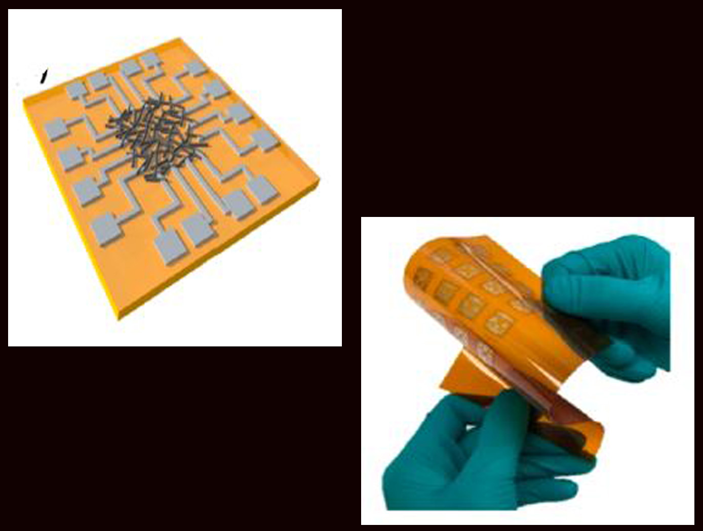
Highly secure all-printed Physically Unclonable Function (PUF) electronic device based on a nanomaterial network
The technology is an all-printed Physically Unclonable Function (PUF) electronic device based on a nanomaterial (such as single-walled carbon nanotube) network. The network may be a mixture of semiconducting and metallic nanotubes randomly tangled with each other through the printing process. The all-printed PUF electronic device comprises a nanomaterial ink that is inkjet deposited, dried, and randomly tangled on a substrate, creating a network. A plurality of electrode pairs is attached to the substrate around the substrate perimeter. Each nanotube in the network can be a conduction path between electrode pairs, with the resistance values varying among individual pairs and between networks due to inherent inter-device and intra-device variability. The unique resistance distribution pattern for each network may be visualized using a contour map based on the electrode information, providing a PUF key that is a 2D pattern of analog values. The PUF security keys remain stable and maintain robustness against security attacks. Although local resistance change may occur inside the network (e.g., due to environmental impact), such change has little effect on the overall pattern. In addition, when a network-wide resistance change occurs, all resistances are affected together, so that the unique pattern is maintained.
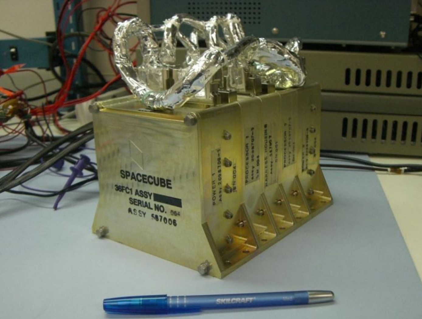
SpaceCube
Next generation instruments are capable of producing data at rates of 108 to 1011 bits per second, and both their instrument designs and mission operations concepts are severely constrained by data rate/volume. SpaceCube is an enabling technology for these next generation missions.
SpaceCube has demonstrated enabling capabilities in Earth Science, Planetary, Satellite Servicing, Astrophysics and Heliophysics prototype applications such as on-board product generation, intelligent data volume reduction, autonomous docking/landing, direct broadcast products, and data driven processing with the ability to autonomously detect and react to events. SpaceCube systems are currently being developed and proposed for platforms from small CubeSats to larger scale experiments on the ISS and standalone free-flyer missions, and are an ideal fit for cost constrained next generation applications due to the tremendous flexibility (both functional and interface compatibility) provided by the SpaceCube system.

Polymer Nanofiber-Based Reversible Nano-Switch/Sensor Schottky Diode Device
Glenn's innovative nanoSSSD device includes a doped semiconducting substrate, an insulating layer deposited on the substrate, an electrode formed on the insulating layer, and at least one polymer nanofiber deposited on the electrode. The deposited nanofiber provides an electrical connection between the electrode and the substrate, serving as the electro-active element in the device. The nanofiber is generally composed of a customized polymer (e.g., polyaniline) that is extremely sensitive to the adsorption and desorption of a single gas molecule. As gas molecules are adsorbed and desorbed, the resistivity of the customized polymer also changes, providing its sensing capacity. When the nanoSSSD device senses a selected gaseous species, the switching portion of the device automatically actuates, sending a signal to the control component. This control component activates the output (warning) device. In addition to its ability to detect harmful gases (including ammonia, hydrogen, hydrocarbons, nitrogen oxides, carbon monoxide, and carbon dioxide), Glenn's device can also feature conducting polymers that are sensitive to UV radiation. Glenn's nanoSSSD technology has great commercial potential, particularly in situations where frequent replacement of the switch/sensor is impractical.

Gated Chopper Integrator (GCI)
The gated chopper integrators function is to amplify low level signals without introducing excessive offset and noise and to do this with accurate and variable gain. The unique feature of the technology is the inherent demodulation present in the integrator which eliminates the need for filtering and allows the user to accurately vary the gain in finely graduated steps. The reduction of the offset of the amplifier is very efficient and lends itself to radiation hardened by design implementations. Since total dose can change the offset due to varying threshold voltages of CMOS transistors, the circuit adapts and compensates for any variations. The autozero integrator also adapts to its own varying offsets. The net outcome is variable, accurate gain that is very robust to supply variations, radiation effects and aging.
The technology was developed as a multi-channel thermopile signal processor. Lab measurements indicate very accurate amplification with low offset and noise.
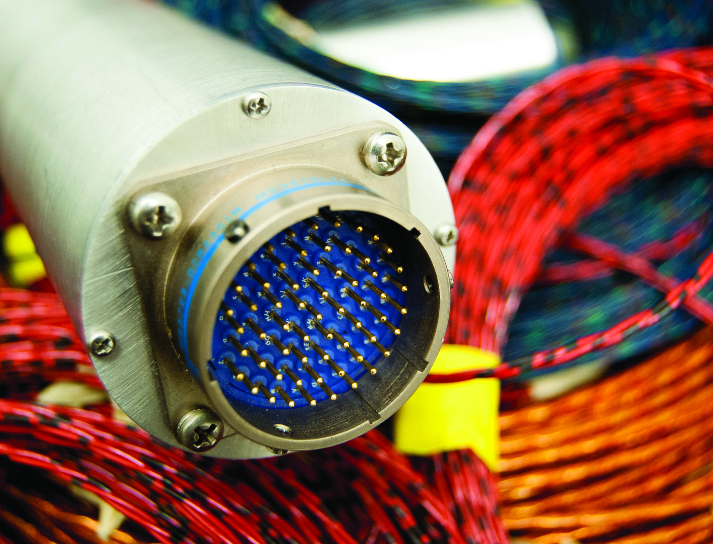
In Situ Wire Damage Detection and Rerouting System
The tester was designed to monitor electrical faults in either online or offline modes of operation. In the online mode, wires are monitored without disturbing their normal operation. A cable can be monitored several times per second in the offline mode, and once per second in the online mode. The online cable fault locator not only detects the occurrence of a fault, but also determines the type of fault (short/open/intermittent) and the location of the fault. This enables the detection of intermittent faults that can be repaired before they become serious problems. Since intermittent faults occur mainly during operations, a built-in memory device stores all relevant fault data. This data can be displayed in real time or retrieved later so maintenance and repairs can be completed without spending countless hours attempting to pinpoint the source of the problem.
Hardware and algorithms have also been developed to safely, efficiently, and autonomously transfer electrical power and data connectivity from an identified damaged/defective wire in a cable to an alternate wire path. This portion of the system consists of master and slave units that provide the diagnostic and rerouting capabilities. A test pulse generated by the master unit is sent down an active wire being monitored by the slave unit. When the slave unit detects the test pulse, it routes the pulse back to the master unit through a communication wire. When the master unit determines that a test pulse is not being returned, it designates that wire as faulty and reroutes the circuit to a spare wire.

Using the Power Grid for Geophysical Imaging
This technology utilizes the U.S. high-voltage power transmission grid system as an extremely large antenna to extract unprecedented spatiotemporal space physical and geological information from distributed GIC observations. GICs are measured using differential a magnetometer technique involving one fluxgate magnetometer under the transmission line and another reference magnetometer station nearby. The reference station allows subtraction of the natural field from the line measurement, leaving only the GIC-related Biot-Savart field. This allows inversion of the GIC amplitude. The magnetometer stations are designed to operate autonomously. They are low-cost, enabling large scale application with a large number of measurement locations.
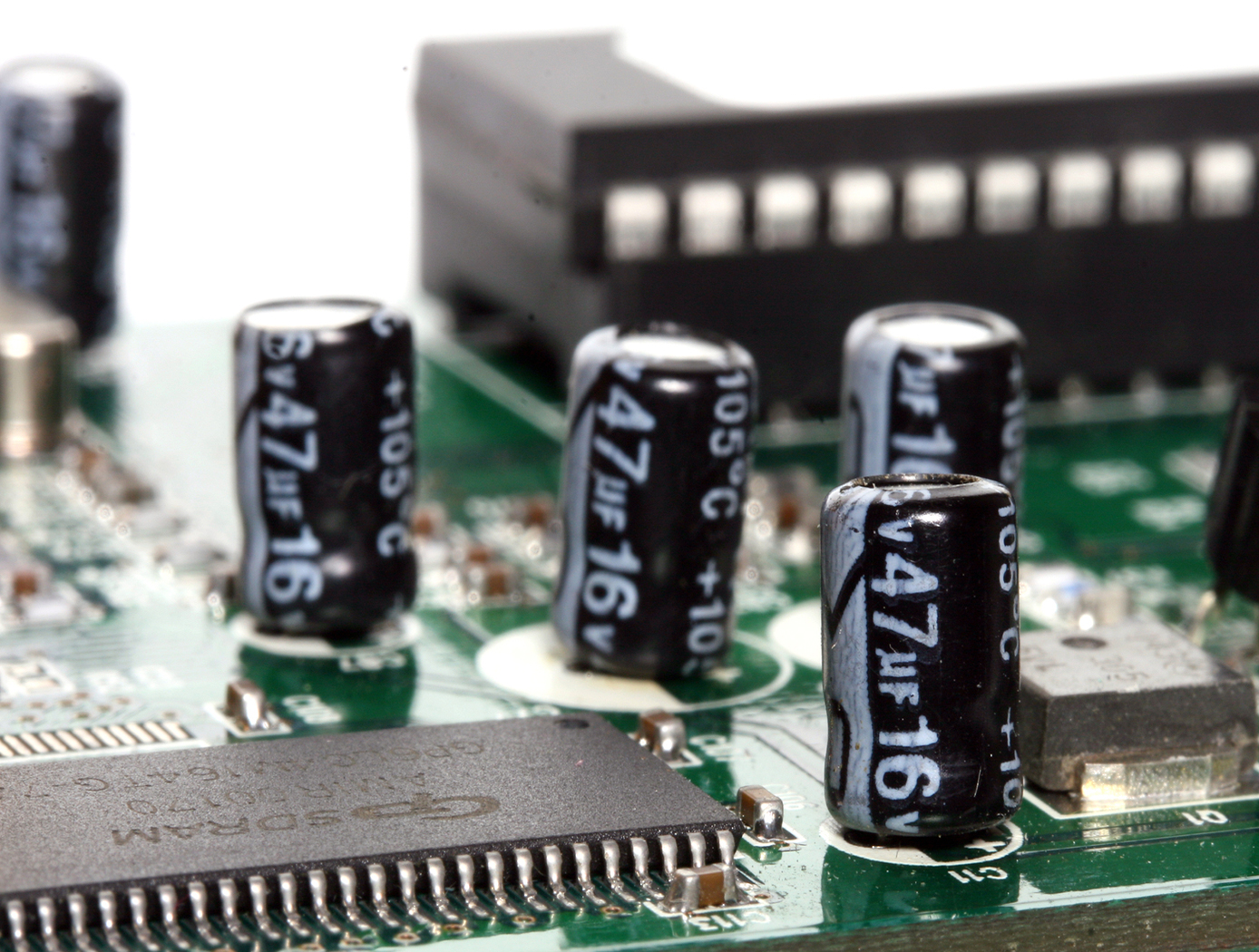
Metal Oxide-Vertical Graphene Hybrid Supercapacitors
The electrodes are soaked in electrolyte, separated by a separator membrane and packaged into a cell assembly to form an electrochemical double layer supercapacitor. Its capacitance can be enhanced by a redox capacitance contribution through additional metal oxide to the porous structure of vertical graphene or coating the vertical graphene with an electrically conducting polymer. Vertical graphene offers high surface area and porosity and does not necessarily have to be grown in a single layer and can consist of two to ten layers. A variety of collector metals can be used, such as silicon, nickel, titanium, copper, germanium, tungsten, tantalum, molybdenum, & stainless steel.
Supercapacitors are superior to batteries in that they can provide high power density (in units of kw/kg) and the ability to charge and discharge in a matter of seconds. Aside from its excellent power density, a supercapacitor also has a longer life cycle and can undergo many more charging sequences in its lifespan than batteries. This long life cycle means that supercapacitors last for longer periods of times, which alleviates environmental concerns associated with the disposal of batteries.
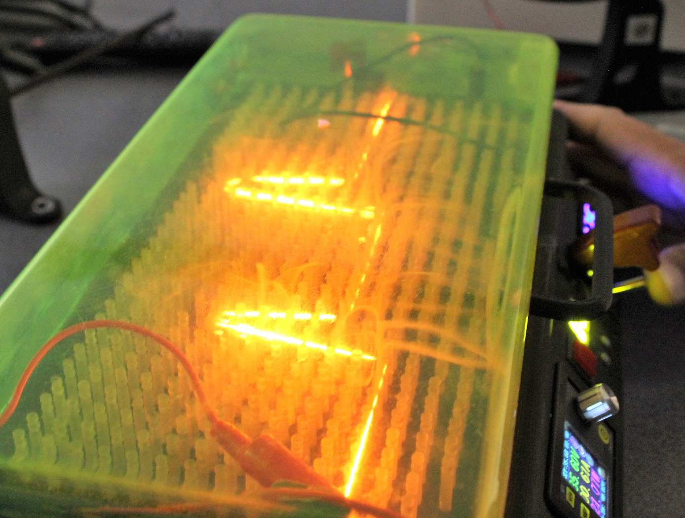
Shape Memory Alloy Art (SMArt)
A prototype device has been developed at Glenn for creating shapes from SMA wire. The apparatus uses material feedstock in spools made of alloys that exhibit the shape memory effect (temperature-induced activation), super elasticity (stress-induced activation), and to some extent, magnetism (magnetically-induced activation). The feedstock (e.g., wire spool) is routed and positioned around a series of modular pins to create a shape outline. Once the desired shape is formed, the wire ends are clipped from the feedstock and secured into a locking mechanism, then connected to a heating circuit (e.g., joule heating, hot plate, heat gun). The programmable prescribed circuit parameters, including current or temperature and training time, are set and confirmed using the apparatus control dials and indicators to ensure safe and accurate operation of the device. Before enabling the circuit, a plastic shield is placed over the modular array to protect the operator. The final product will be a desired shape that can be deformed and recovered numerous times through heat activation.

Serial Arrayed Waveguide Grating
Serial Arrayed Waveguide Grating enables higher resolution wavelength separation. Traditional AWGs split the optical signal into multiple parallel paths each with a different path length. This new approach creates the different path lengths by splitting the signal into essentially one long path in which the different channels are periodically split off the main path in the desired fraction. This has the net result of requiring much less space on-chip for comparable optical path differences.
In traditional AWG, there are multiple parallel optical paths, each with a different engineered path-length. For high resolution, you want many different parallel paths and large differences in path length between the paths. To design this on a photonics chip requires significant area. The serial AWG creates a single path, equivalent to the longest path in the parallel AWG and split off fractions of the optical signal at various points along the way to create the equivalent path lengths. Serial Arrayed Waveguide Grating re-uses the same path instead of needing independent parallel paths.
View more patents


