Search
Manufacturing

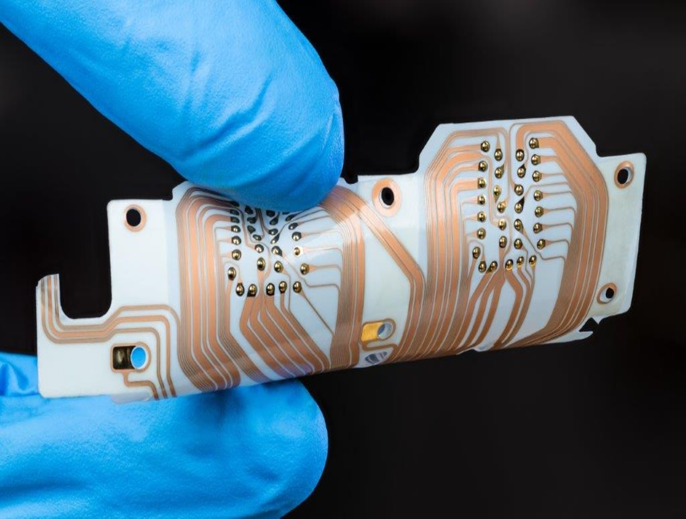
Automated Fabric Circuit and Antenna Fabrication
Modern production of e-textiles utilizes an embroidery technique called “e-broidery” that directly stitches circuit patterns with conductive thread onto textiles. This automated manufacturing process combines steps of e-broidery and milling to expand the application of e-textiles to high-current and high-speed uses. Manufacturing begins with two layouts of the desired conductive pattern. After assembling the layers of conductive and nonconductive materials, e-broidery is performed with the second layout and nonconductive thread to secure the layers together and designate the pattern for the conductive material. The secured assembly is transferred to an automated milling or laser cutting machine, which cuts the desired conductive pattern and releases the unneeded portions of the conductive material. The resulting e-textiles are tightly woven together, providing higher surface conductivity and impedance control. Initial comparison tests assessing the performance of fabric-based spiral antennas developed with this method, compared to conventional antennas, indicated no loss in performance across multiple metrics, including voltage standing wave ratio (VSWR), radiation pattern, and axial ratio performance.
The Method and Apparatus for Fabric Circuits and Antennas is a technology readiness level (TRL) 6 (system/subsystem prototype demonstration in a relevant environment). The innovation is now available for your company to license. Please note that NASA does not manufacture products itself for commercial sale.
Electrical and Electronics

Broadband Metamaterial Termination for Planar Superconducting Transmission Line Circuits
The broadband metamaterial termination for use in planar superconducting transmission lines has been successfully demonstrated in CLASS circuit structures as an effective termination. This metamaterial implementation is fully compatible with microfabrication techniques commonly used for microwave circuitry, and its response is insensitive to geometric tolerances, material properties, and interface details of conductive elements in device fabrication. In the context of far-infrared imaging, polarimetric, and superconducting integral field unit (IFU) spectrometer arrays for astrophysics, this strategy leads to higher performance, increased device yield, and greater overall circuit density.
The metamaterial termination achieves a broadband absorption response with lower reflectance in a smaller physical footprint compared to existing adiabatic structures. This absorption response demonstrates significantly lower sensitivity to fabrication tolerances, material properties, and modeling assumptions than previous designs. These characteristics are critical for cryogenic applications, but the termination can also enhance the performance of room-temperature planar transmission line structures used in microwave engineering. The termination is realized as a lossy stepped impedance transition between Nb and PdAu, which reduces the total meander length, device footprint, and sensitivity to detailed implementation.
This broadband metamaterial termination is applicable in superconducting technologies, including quantum communications, computing, and sensors. It has reached Technology Readiness Level (TRL) 7 (technology demonstrated in an operational environment) and is now available for patent licensing.
manufacturing

Fabricating printable electronics and biosensor chips
The plasma system consists of a glass tube with a diameter of 0.5 mm or larger, if desired. The electrodes are separated by 10 mm. Helium, argon or cold dry air can be used as a plasma gas source. An applied high voltage between the electrodes causes the gas to breakdown within the central core of the glass capillary generating atmospheric plasma. Nanostructures colloids/organic/inorganic precursors are placed in a glass container with an inlet and outlet for carrier gas and are seated on an ultrasonic nebuliser. The aerosol is then carried into the plasma stream by the carrier gas and is deposited.
The atmospheric plasma deposition system can be modified for depositing multiple materials, either simultaneously or sequentially, and for high-throughput processing by having multiple jets. Each capillary can either be connected to the container containing a single precursor material or to different containers containing different precursor materials to facilitate multiple depositions. The multi-jet plasma system can be automated and controlled individually to precisely control surface characteristics. This technique is independent of the chosen substrate, and has proven to work for many substrates, including paper, plastic, semiconductors and metals.
electrical and electronics
Printable IoT sensor development platform
Advances in additive manufacturing have enabled development of printable electronic sensor elements that can be deposited onto flexible substrates. To benchmark performance of printed sensors against the state of the art, NASA developed a low power flexible sensor platform. The platform integrates the following key components and features:
-Flexible substrate: DuPont Kapton allows bending around cylindrical surfaces as small as in diameter.
-Embedded microcontroller: Cypress CY8C4248 LQI-BL583 Arm Cortex M0 processor with BLE wireless controller, max frequency 48 MHz. Supports low power modes of operation, capacitive sensing support, and a single-channel 12-bit AD converter.
-Commercial sensor suite: Bosch BNO080 inertial sensor; Bosch BME280 humidity, pressure, and temperature sensor; AMS CCS811 air quality sensor (VOCs and CO2).
-Prototyping area for custom-printed sensors: 1) thermistor, uses carbon-based PTC resistor paste DuPont2792; 2) capacitive humidity sensor using a NASA-developed dielectric ink.
NASA researchers have used the platform to study performance of the printed capacitive humidity sensor. The 2x4 mm co-doped barium titanate sensing element is highly sensitive to water vapor and performs as an unobtrusive breathing monitor, sensitive to breath at distances of up to 20 cm. Average change of sensor capacitance at a distance of 7.5 cm was observed to be 6.23.5 pF.
Communications

High Performance, All-Metal X-Band Patch Antenna
The patch antenna consists of two radiating metal patch elements, a metal feed circuit, choke rings, several alignment spacers, a SMA connector, and a mounting lid giving the antenna a total diameter of 54 mm; small enough to fit in a coffee cup. The signal is carried between the lower patch and the circuit via a coaxial transmission structure, in which the probes are the inner conductor and the antenna structure is the outer conductor. The patch antenna is constructed entirely of metal, offering rugged physical durability while delivering superior performance. This advanced material not only enables the antenna to handle higher power loads (exceeding 10 watts) but also ensures exceptional stability under demanding conditions—outperforming standard patch antennas made with traditional dielectric materials. It is also not susceptible to the manufacturing variability incurred from using dielectrics. Ideally, this metallic design also allows for reentry and reuse across missions.
The patch antenna is designed with integrated choke rings to effectively mitigate multipath signal interference, delivering an impressive front-to-back ratio of over 35 dB. Its integrated polarizer circuit enhances signal clarity and boosts overall efficiency, ensuring reliable communication in challenging environments. With support for both right- and left-handed circular polarization, the antenna achieves a co-polarization peak gain of 9 dBi and an axial ratio of less than 3 dB within a wide 50-degree orientation range. These advanced features provide superior signal performance and consistent clarity across diverse applications.
Although designed for space and planetary exploration applications, the antenna may also be valuable for terrestrial use cases with rugged conditions. The X-band patch antenna is at technology readiness level (TRL) 5 (component and/or breadboard validation in relevant environment) and is available for patent licensing.
Power Generation and Storage

Ram-Dent Thermal Runaway Triggering Device
The Ram-Dent Thermal Runaway Triggering Device is capable of trig-gering mild short circuits that are similar to internal defects, and more extreme short circuits that are comparable to those initiated by an implanted internal short circuit device – all without having to modify the battery cell in any way. The device imparts a high velocity, low mass blunt impact onto a small surface area of a Li-ion battery cell can wall allowing a small hemispherical dent to form. This impact deforms and tears the internal separator of the battery cell, causing a short circuit, and induces thermal runaway.
Several methods for initiating TR on demand currently exist, but they have characteristics and biases that make them more unfavorable for certain testing objectives. Heat-based insult in any form requires additional thermal energy to be applied to the battery cell, potentially distorting the signal-to-noise ratio in FTRC measurement, and increas-ing the severity of failure beyond what is intended. This methodology also requires time to heat the battery cell to critical temperature, and it potentially weakens the battery cell can wall causing abnormal kinetics and rupture. Mechanical insult methodologies, such as crush testing and nail penetration, have unique applications but rely on deformation of the battery cell itself which alters the flow characteristics of internal gases and the material integrity of the battery cell.
This technology aims to solve these limitations by implementing a cost-effective method to create a natural short circuit failure in Li-ion batteries that does not alter nominal vent paths and energy yields, potentially yielding the most unbiased calorimeter tallies yet.
The Ram-Dent Thermal Runaway Triggering Device is at a technology readiness level (TRL) 4 (component and/or breadboard validation in laboratory environment) and is now available for patent licensing. Please note that NASA does not manufacture products itself for commercial sale.
Electrical and Electronics

Passive PCB-Mounted Thermal Switch
NASA’s Passive PCB-Mounted Thermal Switch uses a heat pipe that extends from the electronics enclosure wall to the center of the electronics board. The switch includes a wax actuator that extends when warm. The extending piston on the actuator pushes the heat pipe against the anvil of the mechanism, which then provides a low-resistance heat path to the wall of the enclosure. When the wax actuator drops below a certain temperature, the piston retracts. A spring then pushes the heat pipe away from the anvil, breaking thermal contact and conserving heat. A series of insulating materials is used to reduce unwanted heat transfer through the springs. The mechanism is mounted to the board with a thermal interface material and screws to provide high contact pressure and thermal conductivity between the board and the mechanism. Additional heat straps are used to carry heat directly from particularly hot components.
A key advantage of this NASA invention is that it does not require any energy input for operations (i.e., it is completely passive). In spaceflight applications, this enables significant mass savings as heaters can represent up to 50% of electronics systems’ power consumption. Given that typical battery chemistries stop functioning at approximately 0C, additional power is required to keep the batteries themselves warm. Thus, reducing heater power requirements by 50% could reduce overall energy storage requirements by approximately 70% – leaving more capacity for sensors, fuel, or other priorities.
NASA’s switch is particularly useful for spaceflight applications where electronics are exposed to long bouts of extreme heat and cold, such as on the Moon (where the day-night cycle lasts 14 days with nighttime lows near -173C and daytime highs near 127C), or in deep space. Lunar landers and lunar infrastructure developers might be ideal end-users of the invention. Other applications where electronics experience extreme temperatures may benefit from this NASA innovation.
Communications

Conformal, Lightweight, Aerogel-Based Antenna
This CLAS-ACT is a lightweight, active phased array conformal antenna comprised of a thin multilayer microwave printed circuit board built on a flexible aerogel substrate using new methods of bonding. The aerogel substrate enables the antenna to be fitted onto curved surface. NASA's prototype operates at 11-15 GHz (Ku-band), but the design could be scaled to operate in the Ka-band (26 to 40 GHz).
The antenna element design incorporates a dual stacked patch for wide bandwidth to operate on both the uplink and downlink frequencies with a common aperture. These elements are supported by a flexible variant of aerogel that allows the material to be thick in comparison to the wavelength of the signal with little to no additional weight. The conformal antenna offers advantages of better aerodynamics for the airframe, and potentially offers more physical area to either broadcast further distances or to broadcast at a higher data rate. The intended application for this antenna is for UAVs that need more than line of sight communications for command and control but cannot accommodate a large satellite dish. Examples may be UAVs intended for coastal monitoring, power line monitoring, emergency response, and border security where remote flying over large areas may be expected. Smaller UAVs may benefit greatly from the conformal antenna. Another possible application is a UAV mobile platform for Ku-band satellite communication.
With the expectation that 5G will utilize microwave frequencies this technology may be of interest to other markets outside of satellite communications. For example, the automotive industry could benefit from a light weight conformal phased array for embedded radar. Also, the CLAS-ACT could be used for vehicle communications or even vehicle to vehicle communications.
mechanical and fluid systems

Additively Manufactured Oscillating Heat Pipe for High Performance Cooling in High Temperature Applications
The advent of additive manufacturing makes available new and innovative integrated thermal management systems, including integrating an oscillating Heat Pipe (OHP) into the leading edge of a hypersonic vehicle for rapid dissipation of large quantities of heat. OHPs have interconnected capillary channels filled with a working fluid that forms a train of liquid plugs and vapor bubbles to facilitate rapid heat transfer. Multiple additive manufacturing techniques may be used, including powder bed fusion, binder jetting, metal material extrusion, directed energy deposit, sheet lamination, ultrasonic, and electrochemical techniques. These high performance OHPs can be made with materials such as Refractory High Entropy Alloys (RHEAs) that can withstand high temperature applications. The structure of the OHP can be integrated into the constructed leading edge. The benefits include a heat transport capacity of 10 to 100 times greater than before. Integrated OHPs avoid the bends or welds in traditional heat pipes, especially at the locations where the highest thermal stresses might cause thermal-structural failure of a leading edge. Alternating the diameters of the OHP channels alleviate start-up issues typically found in liquid metal oscillating heat pipe designs in high temperature applications by aiding in the instigation of a circulating flow due to multiple forces acting upon the working fluid.
Power Generation and Storage

Triggering Li-ion Battery Cells with Laser Radiation
This technology is based upon a 120-watt IR laser is coupled to a fiber optic cable that is routed from the output of the laser into a series of focusing optics which directs energy onto a battery cell mounted to a test stand. When activated, heat from the laser penetrates the metal housing, heating the internals of the cell. At a specific temperature, the separator in the first few layers of the cell melts allowing the anode and cathode to make contact and initiates an internal short circuit. The internal short circuit then propagates throughout the battery eventually causing thermal runaway. The lower the wavelength of the laser used to produce the thermal runaway, the more heat-energy will be absorbed into the cell producing a faster result. The fiber optic cable can be terminated into a series of optics to focus the laser at a specific target, or the fiber optic cable can be stripped bare and placed next to the target to heat an isolated location. This method can also be used on a wide variety of cells, including Li-ion pouch cells, Li-ion cylindrical cells and Li-ion Large format cells.
The innovation Triggering Li-ion Cells with Laser Radiation is at TRL 6 (which means a system/subsystem prototype has been demonstrated in a relevant environment) and the related patent application is now available to license and develop into a commercial product. Please note that NASA does not manufacture products itself for commercial sale.

